Digital imaging research seen as key
in industry
BY DAVID F. SALISBURY
A new Stanford/industry project aims
to make it faster, easier and cheaper to create high-quality pictures electronically.
The project "has the potential to make a significant difference in the
way we capture, store, manipulate and print images," says James Gibbons,
special counsel for industry relations in the President's Office at Stanford,
who helped put the $4 million, three-year deal together.
Related Information:
The project's focus is the development
of innovative designs for the imaging sensor, the electronic chip that
turns patterns of light into digital information. This initial "image capture"
step is of primary importance to the entire digital imaging system, which
has become big business in the last few years. According to a recent marketing
study, revenue from digital imaging products including cameras, camcorders,
scanners and printers was $1.5 billion last year and is projected
to grow to $2.9 billion in 2001.
Industry leaders that have made significant
investments in Stanford's programmable digital camera program include Canon
Inc.; Eastman Kodak Co., Hewlett-Packard Corp., Intel Corp. and Interval
Research Corp.
The Stanford team is applying the latest
in advanced electronics including pixel-level processing - as well
as optics and image science, to design advanced imaging chips. The industry
partners will assist in design and prototyping, and will fabricate chips
for test purposes.
Current electronic imaging systems,
called charge-coupled devices or CCDs, produce analog signals that are
digitized converted to strings of 1's and 0's by a special
purpose chip. The new imaging system, by contrast, integrates digitization
with the image-capture process by moving it to the pixel level. Stanford
has taken out four patents on different aspects of pixel-level processing.
"Pixel-level processing provides a
number of potential advantages," says Abbas El Gamal, associate professor
of electrical engineering, who is the project's principal investigator.
Those advantages include a dynamic range large enough to capture details
of objects in bright sunlight and deep shade at the same time; reduction
in noise; and pixel-level programmability, which could aid in processes
like automatic image recognition.
In addition, the new imaging chip is
made from CMOS, the same technology used to make low-power computer chips.
This allows engineers to combine the imaging sensors with computer circuitry,
reducing the chip count and cutting production costs. Also, because the
pixels in CMOS imaging arrays are "read out" in parallel, row by row, they
are much faster than CCD arrays that read out pixels sequentially. A number
of companies are actively developing analog CMOS imaging chips.
El Gamal sees a range of applications
for the programmable imaging chip that extend beyond basic photography,
applications in which digital imaging has more intrinsic advantages. One
example might be a recognition system for automatic teller machines. The
imaging chip could be programmed to capture just those aspects of an individual's
face that provide positive identification, he says.
Industry interest
The range of companies that are supporting
the Stanford effort suggests how widespread its impact may be, Gibbons
says. Hewlett-Packard sees digital image capture as a natural complement
to their printer business. Kodak recognizes that it will have a significant
impact on its digital and conventional photo operations. Intel envisions
it as one of the next large users of silicon. Interval is interested in
video applications.
Last July, HP's chief executive, Lewis
Platt, told Business Week magazine that the company is betting that
digital imagery "will fundamentally change the way people think about photography"
and that this will allow the electronics company to carve a chunk out of
the $40 billion per year photography market. The potential for producing
substantially improved digital cameras was what attracted the company to
the Stanford project, says Jim Duley, strategic analysis manager for HP
Labs. "We are looking at this as a potentially revolutionary way to capture
images, and we expect to supply the world with the printers to print them,"
he says.
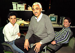
ABBAS EL-GAMAL, ASSOCIATE PROFESSOR
OF ELECTRICAL ENGINEERING, center, works on designing advanced imaging
chips with graduate student David Yang, left, and research associate Boyd
Fowler.
"Stanford's approach is intriguing,"
says Les Moore, manager of digital camera advanced development at Eastman
Kodak. "They are attacking the problem of designing a single-chip digital
camera from a very broad systems perspective. They have one group actively
designing silicon chips and another group modeling the entire imaging system.
That's unique."
David E. Liddle, president and CEO
of Interval Research, says, "We believe that video will play a key role
in the development of intelligent systems in the coming decades. To that
end, we are conducting research designed to improve the capability to process
video data in real time as it is captured. This dovetails with one of the
goals of the Stanford Digital Camera Project, which is to develop architectures
and algorithms for silicon implementation that combine image capture and
image processing."
Intel Corp. recently created a new
business division specifically focused on digital imaging and video. "Intel
believes that there is a strong future in digital imaging and video, and
we offer a variety of technologies and products in this area," says Ray
Hirt, who oversees Intel's participation in the Stanford project. "Our
objective is to provide people with easy-to-use and affordable methods
to capture, enhance, store and deliver high-quality digital imagery. El
Gamal's research is exploring an area that the industry needs to understand
better to move forward on this front."
Started in 1993
The origins of the programmable digital
imaging chip date back to 1993, when El Gamal and graduate student Boyd
Fowler, now a research associate at Stanford, were looking for something
interesting to do with CMOS imaging sensors. After considering a number
of different projects, they hit on the idea of moving the process of digitizing
the electrical signals produced by the image sensors (a process called
"analog to digital conversion," or ADC) onto the chip itself. Currently,
the signals from the thousands or millions of individual sensors on the
chip are collected into a single stream before they are digitized.
"At first this seemed like a crazy
idea because ADC chips are very complex and require a large number of transistors,"
says El Gamal. "But we persisted and figured out a way to do it using very
few transistors per pixel."
After completing a prototype chip,
however, the researchers thought they had reached a dead end. So they turned
their attention to learning more about CMOS imaging sensors themselves.
Much research has been done on these devices, but almost all of it behind
closed doors in industry laboratories. The scientists could find very little
information about the sensors in the technical literature, so they decided
to duplicate all of the commercial sensors on a single chip. This would
allow them to easily compare their physical and electrical characteristics.
About two years ago, industry interest
in image sensors surged. "When corporate engineers began searching the
web looking for people doing research on image sensors they found us. So
we started to get a number of unsolicited inquiries," El Gamal says.
Soon these inquiries were followed
by offers of funding. Several companies, including Intel, Hewlett-Packard,
Rockwell and Analog Devices, gave the researchers substantial grants in
return for use of their image sensor test set. This allowed the researchers
to support their work for several years without having to apply for government
funding.
Industry interest also spurred them
to revisit the issue of pixel-level digitization. Joined by graduate student
David Yang, they came up with a new architecture that promised a number
of advantages. "We realized that we could get enhanced dynamic range and
could also get control of all the parameters, instead of being limited
to the few adjustments you can make with CCD arrays," El Gamal says.
El Gamal met Brian Wandell, professor
of psychology, and Joseph Goodman, the William E. Ayer Professor of Electrical
Engineering, who are key participants in the new effort, through Stanford's
new Image Systems Engineering program.
"The thing that excites me about this
project," says Wandell, "is that it could lead to a future where cameras
are everywhere, like pencils and notepads are today. Imagine giving your
child a small camera, worn as a button on her shirt, so she can send or
save images of her school day. Or imagine making computer-readable notes
of important documents or business presentations by pointing and clicking
a device the size of a penlight."
Wandell is an expert on human vision.
Over the last five years, with funding from Hewlett-Packard, he has developed
a set of metrics that measure how accurately a digital image will appear
to the naked eye. By simulating the imaging system and the display system,
he can predict the quality of the pictures that an imaging chip with certain
characteristics will produce without having to build the chip. He has been
using this capability to advise El Gamal and his students on the design
of their prototype chips.
At the same time, Goodman, who is an
expert on optics, and several of his students have been investigating ways
to use the chip's programmability to compensate for the imperfections caused
by optical lenses.
With their assistance, El Gamal's group
has finished and begun testing the second version of a third-generation
chip. The 1.2 million transistor integrated circuit has pixel-level digitization
that can be programmed to improve its performance in different environments,
such as outdoor scenes, indoor scenes, pages of text or graphics displayed
on computer screens.
With support from Stanford's Center
for Integrated Systems, El Gamal and his students set up a new sensor characterization
laboratory in the CIS annex. The project caught the eye of Gibbons when
he approved the establishment of the laboratory in his previous position
as dean. When he moved to his current position as special counsel for industry
relations, he volunteered his services to help line up significant industry
support. "This project has exactly the potential that I was looking for,"
he says. SR

|